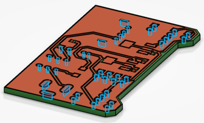
-
From the Create Layout Feature of the action bar,
click Create a hole
 .
.
A specific Hole dialog box appears that contains options
for creating holes on boards with layer stacks.
-
From the Location section, select an X and
Y location and a Rotation value.
-
From the Profile section of the hole editor, choose one of the
following profile types:
-
From the Extremities section, choose one of the following types:
-
Select the placement of the hole within the layers based on the
From and To layers such as:
- BOTTOM_LAYER
- TOP_LAYER
- DIELECTRIC_1
- MIDDLE_LAYER
- DIELECTRIC_2
- BOTTOM_LAYER
The hole is created and appears in the tree.
-
Optional: Select the node to view an outline of the hole.
Holes are now defined while taking the layer stacks into consideration.

