Introduction | ||
| ||
Problem Description
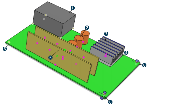
The PCB assembly has a motherboard that is 247 mm long, 146 mm wide, and 2.5 mm tall. The motherboard houses three small capacitors, a power supply (battery), a heat source (main chip), a heat sink, and two small PCBs housing eight small chips. The power supply is connected to the motherboard by point fasteners, while the rest of the parts are connected to the motherboard by tie connections.
The heat sink is made of aluminum, an isotropic and linearly elastic material with a Young's modulus of 70 GPa, Poisson's ratio of 0.35, and density of 2700 kg/m³. The heat source is made of polyimide, an isotropic and linearly elastic material with a Young's modulus of 1.8 GPa, Poisson's ratio of 0.25, and density of 2340 kg/m³. The rest of the parts are PCB substrate, an isotropic and linear elastic material with a Young's modulus of 1.8 GPa, Poisson's ratio of 0.25, and density of 2340 kg/m³.

![]() Power
supply
Power
supply
![]() Capacitors
Capacitors
![]() Heat
sink
Heat
sink
![]() Main chip (heat
source)
Main chip (heat
source)
![]() PCBs
PCBs
![]() Supports
Supports
Workflow
The workflow diagram below provides an overview of the example. The diagram shows the apps that you use as you perform the steps in sequence. Clicking a number in the diagram opens its corresponding step in the example.

| Task | Description | |
|---|---|---|
| 1 | Create the Simulation | Create the simulation by first importing the model into the 3DEXPERIENCE platform and then opening the model in the appropriate app. |
| 2 | Review the Model and Mesh | Review the finite element model (FEM) of the PCB CAD model to assess mesh connections and size. |
| 3 | Create the Analysis Steps | Create analysis steps for the frequency extraction and static preloading analysis steps. |
| 4 | Apply Restraints | Apply restraints to define the directions your PCB can and cannot move during the simulation. |
| 5 | Apply a Translation | Create a load to specify the displacement of the PCB due to manufacturing defects. |
| 6 | Create the Output Requests | Specify the output requests of interest to capture during the simulation. |
| 7 | Run the Simulation | Perform a simulation to extract the natural frequencies on the assembly. |
| 8 | Review the Results | Review the mode shapes of the PCB before and after loading. |
Complete the workflow steps in the order in which they are listed. Deviation from the instructions associated with each step might cause model or scenario errors, which might prevent convergence of the simulation.